Admin
مدير المنتدى


عدد المساهمات : 18739
التقييم : 34745
تاريخ التسجيل : 01/07/2009
الدولة : مصر
العمل : مدير منتدى هندسة الإنتاج والتصميم الميكانيكى
 |  موضوع: كتاب Electrochemistry of Silicon and Its Oxide الجمعة 18 يونيو 2021, 8:13 am موضوع: كتاب Electrochemistry of Silicon and Its Oxide الجمعة 18 يونيو 2021, 8:13 am | |
| 
أخوانى فى الله
أحضرت لكم كتاب
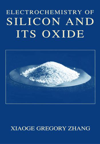
Electrochemistry of Silicon and Its Oxide
Xiaoge Gregory Zhang
Cominco Ltd.
Mississauga, Ontario, Canada
and
McMaster University
Hamilton, Ontario, Canada
و المحتوى كما يلي :
Contents
LIST OF SYMBOLS xxiii
CHAPTER 1. Basic Theories of Semiconductor Electrochemistry
Introduction 1
Energetics of Semiconductor/Electrolyte Interface
Energy Levels in Semiconductor
Energy Levels in Electrolyte
Distribution of Energy Levels in Electrolyte
Energy Levels at Semiconductor/Electrolyte
Interface
Potential and Charge Distribution in Space Charge Layer
Carrier Density in Space Charge Region
Depletion Layer
Accumulation Layer and Inversion Layer
Helmholtz Double Layer
Surface States
Fermi Level Pinning
Equivalent Circuit and Capacitance of
Semiconductor/Electrolyte Interface
Flatband Potentials
Kinetics of Charge Transfer
Basic Theories
Limitations of the Basic Theories
Limiting Current
Breakdown
Potential Distribution
Current Multiplication
Photoeffects
Photocurrent
Photopotential
Efficiency of Energy Conversionxvi CONTENTS
1.5.4. Surface Recombination
Open-Circuit Potential
ExperimentalTechniques
CHAPTER 2. Silicon/Electrolyte Interface
Basic Properties of Silicon
Thermodynamic Stability in Aqueous Solutions
Surface Adsorption
2.3.1. Hydrogen Termination
Mechanistic Aspects
Fluoride Termination
Adsorption of Metal and Organic Impurities
2.4. Native Oxide
In Air
In Water and Solutions
Hydrophobic and Hydrophilic Surfaces
Surface States
Flatband Potentials
Effect of pH
Effect of Surface Condition
Effect of Surface States
Band Diagrams
2.8. Open-Circuit Potentials
2.8.1.
2.8.2.
Effect of Various Factors
Corrosion Current
CHAPTER 3. Anodic Oxide
3.1.
3.2.
Introduction
Types of Oxides
Thermal Oxide
Chemical Vapor Deposition
Liquid-Phase Deposition
Native Oxide and Anodic Oxide
Use of Oxides in Device Fabrication
3.3. Formation of Anodic Oxides
General
Effect of Solution Composition
Effect of Silicon Substrate
Effect of Polarization Conditions
Effect of Illumination
Electroluminescence
3.4. Growth Mechanisms
105CONTENTS xvii
Reactions 105
Ionic Transport within Oxide
Growth on n–Si
Electroluminescence
An Overall Growth Model
Growth Kinetics
Thermal Oxides
Anodic Oxides
3.5. Properties
3.5.1. Physical and Chemical Properties
Interface
3.5.2. Electrical Properties
Thermal Oxides
Anodic Oxides
CHAPTER 4. Etching of Oxides
Introduction
General
Thermal Oxide
Quartz and Fused Silica
Deposited Oxides
Anodic Oxides
Etching Mechanisms
4.7.1.
4.7.2.
4.7.3.
Reactions
In Nonfluoride Solutions
In HF-Based Solutions
Rate Equations
Effect of Oxide Structure
CHAPTER 5. Anodic Behavior
Introduction
Current–Potential Relationship
5.2.1.
5.2.2.
Fluoride Solutions
Effect of Solution Composition
Alkaline Solutions
Photoeffect
5.3.1. Quantum Yield and Surface Recombination
Effective Dissolution Valence
Hydrogen Evolution
Limiting Current
Impedance of Interface Layers
Tafel Slope and Distribution of Potential
193xviii CONTENTS
Tafel Slope
Potential Distribution
Passivation
Occurrence
Passivation in Alkaline Solutions
Passive Films
Current Oscillation
5.10.1.
5.10.2.
5.10.3.
Amplitude and Frequency
Oscillation of Anodic Oxide Thickness and
Properties
Mechanisms
A New Model
5.11.
5.12.
Participation of Bands and Rate-Limiting Processes
Reaction Mechanisms
5.12.1.
5.12.2.
Turner–Memming Model
Later Modifications
Model to Account for Electron Injection into the
Current Band
Modification for Hydrogen Termination
Consideration of Chemical versus Electrochemical
Reaction
Individual Steps in the Transfer of Valence Electrons
5.12.3.
5.12.4.
Models for the Reaction Mechanisms in Alkaline
Solutions
An Overall Reaction Scheme
Elemental Steps
Reaction Paths
CHAPTER 6. Cathodic Behavior and Redox Couples
6.1.
6.2.
6.3.
6.4.
6.5.
Introduction
Hydrogen Evolution
6.2.1.
6.2.2.
Kinetics
Surface Transformation
Metal Deposition
6.3.1.
6.3.2.
Deposition of Silicon
Redox Couples
6.5.1. Individual Redox Couples
Other Redox Species
6.5.2. Electroluminescence Associated with Redox
Reactions
Kinetics
MorphologyCONTENTS xix
6.6.
6.7.
Open-Circuit Photovoltage 268
270
272
274
276
Surface Modification
6.7.1.
6.7.2.
6.7.3.
Metallic Deposits
Polymer Coatings
Nonaqueous Solutions
CHAPTER 7. Etching of Silicon
7.1.
7.2.
7.3.
7.4.
Introduction
General
Fluoride Solutions
7.3.1.
7.3.2.
7.3.3.
7.3.4.
Absence of Oxidants
Effect of
Effect of
Effect of Other Oxidants
Alkaline Solutions
7.4.1.
7.4.2.
7.4.3.
KOH Solutions
Etching Mechanism
Other Inorganic Solutions
Solutions
Hydrazine
Organic Solutions
EDP Solntions
Ethanolamine
Tetramethyl Ammonium Hydroxide (TMAH)
7.5.
7.6.
Etch Rate Reduction of Heavily Doped Materials
Anisotropic Etching
7.6.1.
7.6.2.
7.6.3.
Sensitivity of Etch Rates to Crystal
Orientation
Mechanisms
Rate-Limiting Process
Passivation Models
Surface Reaction Kinetics-Based Models
Mechanism of Anisotropic Etching
Basic Features of Anisotropically Etched
Surfaces
7.7.
7.7.1.
7.7.2.
7.7.3.
Surface Roughness
Microroughness
Macroroughness
Crystallographic Characters and Formation of Hillocks
Origins of Roughness
7.8.
7.8.1.
7.8.2.
Applications
Cleaning
RCA Cleaning
Defect Etching
344xx CONTENTS
7.8.3. Material Removal 347
Uniform Material Removal
Selective Material Removal
CHAPTER 8. Porous Silicon
8.1.
8.2.
Introduction
Formation of Porous Silicon
Characteristics of i–V Curves
Conditions for PS Formation and Electrochemical
Polishing
Effective Dissolution Valence and Hydrogen
Evolution
Growth Rate of Porous Silicon
Mass Transport
8.3 Morphology
General
Diameter and Interpore Spacing
Effect of Doping
Effect of Potential
Primary and Branched Pores
Pore Arrays
Variation from Surface to Bulk
Interpore Spacing
Distribution of Pore Diameter
Pore Density
Pore Orientation and Shape
Pore Branching
Interface between PS and Silicon
Depth Variation
Transitional Layer
Two-Layer PS
Fill of Pores
Density and Specific Surface Area
Composition
Crystallographic Structure
Summary
PS Formed at OCP
PS Formed under Special Conditions
Formation Mechanisms
8.6.1. Historical Development
Discovery of PS and the Initial Model
Macropores on n-Si and the Barrier Breakdown Model
Characterization of PS and Growth Kinetics
Chemical Dissolution during PS FormationCONTENTS xxi
Depletion Layer and Field Intensification Model 410
Carrier Diffusion Model
Formation Condition of PS
Quantum Confinement Model
Surface Curvature Model
Formation of Uniformly Spaced Pore Array
Formation of Two-Layer PS on Illuminated n-Si
Theories on the Macro PS Formed on Lowly Doped p-Si
Miscellaneous Hypotheses
Integration of Models
Current Burst Theory
Advances in the Understanding of Electrochemical
Reactions
Summary
8.6.2. Analysis of the Mechanistic Aspects Involved in PS
Formation
Effect of Radius of Curvature
Potential Drop in the Substrate
Anisotropic Effect
Reactions on the Surfaces of Silicon and Silicon Oxide
Distribution of Reactions and Their Rates on Pore
Bottoms
Dissolution of PS
Potential Drops in Different Phases of the Current Path
Relativity of the Dimensions and Events
Pore Diameter and Interpore Spacing
Varitation of Morphology from Surface to Bulk.
Initiation of Pores
8.6.3. Summary
8.7. Properties and Applications
CHAPTER 9. Summaries and General Remarks
Complexity
Surface Condition
Oxide Film
Sensitivity to Curvature
Sensitivity to Lattice Structure
Relativity
Future Research Interests
REFERENCES
INDEX
x
Absolute scale, 6, 8, 9
Absorption, 3, 8
hydrogen, 242
hydroxyl, 141
light, 3, 8, 14, 31, 212, 415
Acceptor, 2, 21
Accumulation layer, 10, 11, 14
photo potential, 35
Acetic acid, 252, 290
Acetonitrile, 16, 75, 79, 276
Acids, 86, 179
Activation energy
etching of silicon, 280, 284, 290, 305, 317, 319
etching of oxide, 132, 137, 159
hydrogen termination, 59
Adsorption, 53–63, 154
fluoride, 60, 158
Helmholtz layer, 13, 153
hydrogen, 55–60, 75
hydroxyl, 61, 152, 158
organic, 61, 63, 69
other species, 61
oxide surface, 156, 158
water, 53, 152
Aeration, 40
Aging, 65, 70, 215
Air, 63
Air bubbles, 141
Alcohols, 63, 106, 296
Alignment, 315, 324
Alkali, 144, 154, 198
Alloying, 146, 164, 294
Aluminum, 294, 306
Amine, 305
Ammonia, 63, 87, 276
Amorphization, 241
Amorphous phases, 52, 242, 287, 400, 448
Analytical techniques, 41
Angle, 315, 322
Anisotropic etching, 280, 295, 312–323, 423, 448
etched feature, 323
mechanism, 316, 448
Annealing, 120, 123, 128, 148
Anodic dissolution, 167, 218, 229, 354
characteristics, 169, 170, 229
illumination, 168
mechanism, 219, 229
potential, 168
solution composition, 168
type of silicon, 168
uniformity, 229, 355
Anodic oxides, 91, 115, 125, 148, 201, 444
breakdown potential, 125
coverage, 242, 247, 249, 425, 437, 444
current oscillation, 210–212, 215
dissolution, 229, 446
electric properties, 122, 125
etching; see Etching of oxides
formation, 94, 174, 446
current efficiency, 95, 98, 100
field strength, 115
illumination, 103, 108
maximum potential, 95
n-Si, 108
solution composition, 96
yield, 95, 103, 202
formation mechanism, 105–112
growth kinetics, 112, 115–116
impedance, 189
impurities, 118
localized states, 112
luminescence, 104, 109
passive films, 201, 444
passivation 167, 174, 195
physical properties, 116, 118, 211
porous silicon, 357, 366, 399, 425
structure, 118, 126–130, 150, 163
thickness, 204, 210, 215
499500 INDEX
Anodization
electropolishing, 169, 354
etching, 348
formation of oxide, 94, 195
formation of porous silicon, 169, 354
Area, 88, 102, 242, 327, 354, 396
Aspect ratio, 351
Atomic density, 45
Avalanche breakdown, 27, 108
Back-bonds, 59, 106, 226, 287, 320
Band diagram, 2, 3, 82, 111, 275
Background light, 36
Band edge, 7, 9, 18, 23, 268
Band gap, 2, 46
charge transfer, 22
photo effect, 31, 36, 174
surface states, 15, 75
Band bending, 3, 10–13, 217, 229, 432
equilibrium, 23
flatband,8
photo current, 34, 174
photo potential, 36, 268
surface states, 15, 180
Barrier, 68, 108
Barrier height, 245, 273, 416
Bias, 10, 28, 34, 298, 349
Bond strength, energy, 14, 45, 55, 58, 72, 75, 448
anisotropic etching, 319, 320
dissolution reactions, 229
oxide etching, 151, 165
Breakdown, 27–29
oxide film, 98, 125, 213
passivation, 168
silicon/electrolyte interface, 108, 170, 410
Breakdown field, 46, 109, 125
Bubbles, 141, 242, 338, 360, 407
Buffering, 52
Capacitance, 12, 14–18, 189
accumulation layer, 12
depletion layer, 11
double layer, 13
flatband potential, 18–21
Helmholtz layer, 13, 14
inversion layer, 12
oxide film, 123, 128, 189
porous silicon, 354
space charge layer, 9–13
surface states, 15, 72–75, 123
Carriers, electron and hole
charge transfer, 219, 228, 238, 248
distribution, 5
etching, 292, 305, 321
generation, 3, 9, 31, 184, 241, 424
Carriers, electron and hole (cont.)
relation to doping, 5
transport, 216, 447
type, 6
Carrier density, 9
doping effect, 5
intrinsic, 5, 184
photo effect, 32, 36, 424
surface, 23
Carrier transfer; see Charge transfer
Catalytic effect, 174, 239, 292, 306
Cathodic behavior, 237
Cavity, 324, 349
Cell, 37, 407
Ceramics, 54
Charge, 120, 123
distribution, 7, 123
immobile type, 10, 123
mobile type, 123, 128,
transfer, 13
surface states, 15, 120
Charge transfer, 21, 217
coefficient, 30, 194
interface states, 120
involvement of bands, 22, 238
mechanism, 217
metal deposition, 273
polymer coating, 274
redox species, 3, 7
surface states, 15
Chemical etching; see Etching of oxide
Chemical dissolution, 182, 359, 367–368, 428
Chemical potential, 2, 5, 6
Chemical reactions, 23, 226, 229, 248
Chemical vapour deposition, CVD 93
Chemicals, 86, 85, 244, 252
258, 293
CsOH, 144, 298
HC1, 103
HF; see Fluoride
83, 86, 96, 250, 290
96
68, 96, 138, 173
244
139
68, 141, 260, 293, 299, 337
KC1, 73
KF, 142, 155
262, 264
74
155
74
KOH; see KOH
262
79INDEX 501
Chemicals (cont.)
LiOH, 144, 298
NaCl, 72, 97, 144
254, 288
NaOH, 144, 298
301
53, 138
142
107, 298
RbOH, 144, 298
others
Cleanness, 53, 63, 70, 341
Cleaning, 340–344
contamination, 61
hydrogen termination, 55
metal deposits, 248
RCA process, 330, 342
SC-1 solution, 62, 70, 141, 147, 299, 320, 343
surface roughness, 328
surface treatment, 43
Cleavage 63, 67
Coefficients 45
charge transfer 30, 194
diffusion 27, 46
generation and recombination 38
photo absorption 32, 33, 415
potential partitioning 18
Complex, 47, 53, 153, 256
Complexity, 219, 276, 419, 450, 441–444
Conduction band, 2, 217
Contamination, 54, 61, 289, 340
Convection, 40, 366
Copper, 66, 87, 89, 239, 245
Corner undercut, 327
Corrosion, 39–41, 87–90, 246, 250, 347, 428
Coverage, 242, 272, 275
fluoride, 61
hydride, 55, 286, 444
metal deposit, 248
oxide, 58, 423, 433, 444
porous silicon, 354, 423, 437
Crack, 51
Crystal, 45, 46
Crystal structure, 448
oxide film, 92
porous silicon, 399
silicon, 46
Crystal orientation; see Orientation
Current, 22, 168
anodic current, 22–24
cathodic current, 22–24
corrosion current, 39
electropolishing, 357
exchange current, 29
limiting current, 26, 29, 40
Current (cont.)
passivation current, 168, 173, 196
photo current; see Photo current
saturation current, 35
short circuit current, 35, 37
Current burst, 417
Current distribution, 427, 433
Current doubling; see Current multiplication
Current efficiency, 94, 175
Current multiplication, 31, 174, 217, 222
Current path, 428, 434
Current oscillation, 167, 207–216
characterization, 207
impedance, 92
mechanism, 212, 417
oxide properties, 149, 220
Curvature, 420, 446
porous silicon formation, 413, 420
solubility, 51
CVD oxide, 133, 146
Dangling bond, 14, 53
interface states, 120
surface states, 14, 178
Dark current, 27, 120, 184, 241, 268, 273
Deaeration, 41
Debye length, 46
Decomposition
299
solvent molecules, 277, 305
water, 47
Defects, 88, 92, 179, 184, 321, 433
current oscillation, 212
etching, 231, 287, 308, 327, 338, 344–347
hydrogen adsorption, 231
porous silicon, 375, 433
Degenerate doping, 169, 195, 199
Degenerate surface, 11
Delineation, 288
Dendrite, 380
Depletion layer, 10, 28; see also Space charge
layer
anodization of n-Si, 108
photo current, 32
photo potential, 35
Deposition, 62, 81; see also Metal deposits
metals, 243
polymer, 275
silicon, 251
Derivation, 271, 274, 328, 340, 450
Device fabrication, 94, 328, 340, 346, 450
Dielectric breakdown, 27, 109, 125
Dielectric constant, 20, 46, 125
Diffusion, 217, 365
activation energy, 132, 280502 INDEX
Diffusion (cont.)
carriers, 27, 184
coefficient, 36, 113, 119
ionic species, 113
oxygen, 112
process, 19, 114, 212
water in oxide, 108, 114, 119
Diffusion length, 27, 32, 36
Dilution, of solution, 285, 291
Dimension, 429, 442, 449
Dipoles, 122
Dislocation, 14, 263, 345
Displacement reaction, 62
Dissociation constant, 52
Dissolution; see also Anodic dissolution
etching of silicon, 279
OCP, 40, 68
of oxide, 51, 200, 229; see also Etching of oxide
process and mechanism, 219, 229, 312, 420
reactions, 219
valence, 180, 184, 229, 233
chemical dissolution, 182
etching in HF solutions, 288
illumination, 181
potential, 181
PS formation, 359
type of silicon, 181
Dissolution products, 305
Distance, 22, 46, 68
Distribution
Boltzmann distribution, 9, 162
current, 427, 433
energy levels, 6
Fermi Dirac distribution, 4
Gaussian distribution, 7
Maxwell–Boltztnann distribution, 5
metal deposit nuclei, 250
potential and change, 9, 16, 193, 428
reactions, 426, 447
surface states, 15, 37, 73
Donor, 2, 21
Dopant, 45
concentration, 9, 11
energy level, 2
etch stop, 308
type, 164
Doping, effect of concentration
anisotropic etching, 314
band gap, 2
carrier concentration, 5
dissolution valence, 182, 360
electropolishing, 169
etch rate, 182
oxide, 147, 163
silicon, 286, 291, 296, 309, 314
Doping, effect of concentration (cont.)
flatband potential, 75
limiting current, 186
impedance, 190
i-V curves, 169
native oxide, 65
OCP, 83, 86
passivation, 182, 199
photo current, 34
porous silicon, 355, 360, 432
potential distribution, 29
oxide formation, 126
Doping, effect of type
breakdown filed, oxide, 126
current oscillation, 207
etch rate, 297, 302, 306
hydrogen evolution, 183, 241
impedance, 190
i-V curves, 168, 173, 297
leaking current, oxide, 127
metal deposition, 245, 250
oxide growth, 101
passivation, 198
photo current, 175
porous silicon, 355, 359, 432
potential distribution, 195
quantum yield, 178
redox reactions, 254
reaction mechanisms, 219, 229, 432
Tafel slope, 194
Double layer, 3, 4, 13
Earth, 131
Edge
crystal terrace, 320, 321–323
energy bands, 7, 9, 18, 23, 268
wafer, 141
EDP, EPW, 302; see also Etching of silicon
Efficiency
energy conversion, 270
hydrogen evolution, 183, 237
ionic current, 94
redox reaction, 21
photo current, 175
Electrochemical techniques, 42
Electrode
preparation, 43, 60, 340
ring-disc, 183
Electrode potential, effect on
anodic oxide formation, 95
anodic dissolution, 167
current oscillation, 208
dissolution mechanism, 219
etch rate, 293, 297, 302, 304, 308
etch-stop, 349INDEX 503
Electrode potential, effect on (cont.)
passivation, 167
surface roughness, 331
Electroless deposition, 243
Electroluminescence, 104, 109, 266, 437
Electroplating; see Deposition
Electrolyte; see Solution
Electron, 8, 46
Electronic current, 109, 115
Electron transfer; see Charge transfer
Electronegativity, 69, 122
Electropolishing, 169, 182, 190, 356, 430
Emission, of photon, 104, 109, 268
Emmision center, 110
Energy conversion, 37, 273
Energy bands, 2, 216
Energy levels, 4, 6, 7, 46, 217, 319
charge transfer, 21
empty states, 7, 15, 22
occupies states, 7, 15, 22
surface states, 14, 71
Energy overlap, 21
Enthalpy, 344
Epitaxial layer, 63, 342, 345
Equilibrium, 4, 39, 47
carrier distribution, 2
charge transfer, 21
double layer, 13, 153
redox species, 6, 36
surface adsorption, 154, 162
Equivalent circuit, 16
Etch rate, 132, 182
calculation, 288
OCP, 182
oxides, 133, 137, 148, 211
other materials, 283, 294, 306,
silicon, 182
Etch pits, 251, 345
Etchants, 281
alkaline based, 294
KOH, 295
299
EDP, 302, 314
TMAH, 306
anisotropic etching, 312
defect etching, 344
fluoride based, 138, 285
isotropic etching, 256
Etching of oxide, 131, 283, 294
activation energy, 133, 137
anodic oxide, 148, 211
application, 131
cleaning, 70
mechanism, 151
Etching of oxide (cont.)
potential, 141, 150
rate equation, 158
solution composition, 138
structure, 139, 149, 163
type of oxides, 133, 145, 147
Etching of silicon, 279
activation energy, 280, 290, 317
applications, 340
defects, 344
dissolution products, 297, 305
doping effect, 308
effect of orientation, 287, 312–323
etchants; see Etchants
morphological features, 280, 323, 345
OCP, 41, 85
potential, 290, 299, 351
precipitation, 296, 298
reaction mechanism, 292, 297, 310, 316, 446
relative to other material, 133 283, 294, 306
techniques, 348
temperature, 290, 295
time, 295
undercuts, 323
work damaged surface, 292
Etch-back, 120, 204
Etch-stop, 308, 349
Etching techniques, 348
Ethanolamine, 305
Exchange current, 29, 30, 186, 239, 273
Excess charge, 38
Experimental techniques, 41
Faraday’s law, 288
Fermi Dirac distribution, 4
Fermi level, 5
OCP, 39
semiconductor, 2
surface states, 16
pzc of oxide, 120
Fermi level pinning, 16, 20, 80, 269, 417
Fick’s law, 113
Field, 420
breakdown, 28, 125
bulk silicon, 432
carrier separation, 31
limiting current, 186
oxide film growth, 94, 100, 125
space charge layer, 420
Field intensification, 410, 416, 420
Flat band potential, 12, 18–21, 75–82
definition, 8
interface states, 120
luminescence, 267
metal deposit, 272
301504 INDEX
Flat band potential (cont.)
Mott–Schottky equation, 11, 11–20
OCP, 85
oxide film, 21, 125
photo potential, 35
PZC, 9
redox couples, 80
surface states, 19, 21, 128
transient effect, 128
Fluorine/fluoride, 50–53, 168
current oscillation, 237
etching, 137, 155, 285
complex, 48
in oxide, 125, 118
i-V curve, 171
pH, 48
reaction mechanisms, 219, 441
solubility, 50
Fluoride termination, 60, 66, 70
Fractal structure, 432
Frequency, 32, 73, 80
Free energy, 45, 319, 320
Future, 450
Galvanic action, 348
Galvanostatic, 101
Gas, 120
Gassing, 288
Gauss law, 11
Generation center, 241
Geological system, 131, 144
Geometry, 443, 447
etched structure, 152, 323, 335, 348
pores, 434
surface curvature, 51, 420, 446
surface lattice, 321, 335, 423, 446, 448
Glass, 137, 146, 164
Gold, 15, 81, 289
Gouy–Chapman layer, 3
Grain, 272
Heat treatment; see Annealing
Helmholtz layer, 3, 13–21, 26, 193
capacitance, 191
double layer structure, 8, 153
flat band potential, 20
hydrogen evolution, 238
PS formation, 428
surface states, 14, 16, 80
Helmholtz potential, 7, 13, 75
Henry’s law, 113
High field mechanism, 115
Hillocks, 297, 300, 334
History
research progress, 408
History (cont.)
theories on anodic dissolution, 219, 419
Holes density, 9, 23
Hole lifetime, 27
Hole mobility, 45
Hot electron, 109
Hydration, 51, 107, 152
Hydride, 47, 55–60, 242
Hydrogen, 47
absorption, 241
adsorption; see Hydrogen termination
evolution; see Hydrogen reduction
Hydrogen potential, 6
Hydrogen reduction, 237
efficiency, 182
etching, 288, 287, 304
electroluminescence, 267
hydride formation, 242
in passive region, 212
kinetics, 183, 238, 241
mechanism, 58
metal deposition, 245, 272
nature of reaction, 241, 228
porous silicon, 354, 358
roughness, 338
thermodynamics, 47
Hydrogen termination, 55–60, 229, 242, 444
activation energy, 59
anodic dissolution, 222
hydrophobicity, 70
limiting current, 185
native oxide, 63, 67, 69
polymer deposition, 276
porous silicon, 359, 417
surface roughness, 320
surface states, 14, 72
Hydrolysis, 151
Hydrophilic–hydrophobic surface, 65, 70, 251, 444
Hydroxide, 108
Hydroxyl, 107, 141, 150, 297
Hydroxyl termination, 55, 61, 67, 70
Illumination, 174
anodic oxide formation, 103
corrosion, 40, 428, 434
direction, 373, 431
dissolution valence, 181, 184, 358
electroless deposition, 247, 251
etching, 304, 304, 349
hydrogen evolution, 184, 239
i-V curves, 168, 174
OCP, 87, 268
passivation, 174, 206
porous silicon, 358, 365, 389, 434
quantum efficiency, 176INDEX 505
Illumination (cont.)
surface states, 72, 81, 176
wavelength, 33, 177, 432
Impedance, 189
anodic dissolution, 189
oxide film, 128
porous silicon, 354
Impurity, 399
contamination, 61, 340
doping, 45
in oxide, 65, 92, 125, 164
Incubation, 64, 67
Inhibition, 41, 155
Inhomogeneity, 14, 250
Initiation, 254, 433
Interfaces, 189, 194, 204, 218, 266, 429, 441
living mater/non-living mater, 451
metal/electrolyte, 273
112
Si/metal, 273
Si/polymer, 451
Si/porous silicon, 386, 374
15, 77, 107, 111, 124, 120
states, 122, 128, 130
photo current, 174, 206
Si/water, 4, 7, 152, 159, 273, 421
111, 120
Interface tunnelling, 28, 170, 188, 421
Interface states, 15, 120, 128
Intermediates, 223
anodic dissolution, 29, 183, 190
anodic oxidation, 105, 128, 204
current multiplication, 31
etching of oxide, 156
redox reactions, 189
surface states, 14, 74, 185
Intrinsic states, 14, 72
Inversion layer, 10, 36
Ion implantation, 141
anodization, 100
etch rate, 287
Ionic transport, 106, 115, 213
Ionization, 45, 125, 162
Ions, 13, 16, 51
metal ions, 51, 53, 61, 87, 173
Isopropyl alcohol, IPA, 295, 298, 302, 306
Isotope, 106, 156
Isotropic etching, 256, 323, 448
I–V curve, 40, 41, 168, 348, 354
anodic dissolution, 168, 354
anodic oxide film, 125, 127, 426
doping, 171, 173
etching, 293, 297, 302, 304, 308, 348
formation of porous silicon, 169, 426
hydrogen evolution, 238
I–V curve (cont.)
metal deposition, 245
organic solutions, 276
passivation, 168, 173
redox couples, 254
Kinetic energy, 28
Kink, 14, 45, 55, 320
Knowledge base, 450
KOH
dissolution valence, 182
etching of oxide, 140
etching of silicon, 294
etching of quartz, 144
passivation, 173
reaction mechanism, 225
roughness, 332
Langmuir adsorption model, 62
Laser, 348
Lattice constant, 45, 46
Lattice structure, 45, 321, 335, 399, 443, 448
Leakage current, 125, 127, 340
Lewis sites, 14
Lifetime, 33, 46
Ligands, 158
Light; see Illumination; Photo effect
Limiting current, 27, 29, 40, 184
Luminescence, 104, 108, 266
Marker, 106
Mass transport, 354, 358, 365–367, 414
Mask, 190, 294, 313, 324, 327, 407
Maxwell–Boltzmann distribution, 5
Mean free path, 109, 125
Measurement, 39, 42, 355, 441
anisotropic etching, 313
etch rate, 132
surface roughness, 327
Mechanisms, 219–235, 408–440, 442
anisotropic etching, 316–323
anodic reactions, 219
charge transfer, 217
current oscillation, 212–216
dark limiting current, 184
electroluminescence, 267
etching of oxide, 151–165
etching of silicon, 297, 310
formation of porous silicon, 408–437
formation of anodic oxide, 104–112
heavy-doping etch stop, 310
hydrogen termination, 58
native oxide, 64, 69
passivation, 234
redox reactions, 254
surface roughness, 338
Metallic behavior, 11, 265506 INDEX
Metal deposits, 240, 270
catalyst, 240, 270, 273
cleaning, 341, 344
etching, 312
hydrogen evolution, 239, 245
surface contamination, 53, 61, 66, 81, 180
Methanol, 79, 97
Micro domain, 212, 214
Micromachining, 131, 294, 340, 350
Microwave, 212
Minerals, 132, 154
Mixed potential, 8, 39
Mobility, of carriers, 46
Monomer, 51
Morphology, 248, 327, 368
anodic dissolution, 169
cleaned surface, 341
etched surface, 143, 287, 280, 296, 327
metal deposits, 247
porous silicon, 368, 433
Mott–Schottky equation, 12, 19, 189, 274
flatband potential, 19
Helmholtz layer effect, 13
plot, 19, 81
Multiplication, 28, 31, 175
Native oxide, 63, 444
adsorption, 53, 62
in air, 63
cleaning, 43, 344
passivation, 67
in water, 67
Nernst equation, 6
Nickel, 247
Nucleation
hillocks, 337
metal deposits, 247
pores, 375, 433
steps, 320, 322
surface oxide, 64, 67
Nuclei, 249
Ohmic contact, 274
Ohmic effect, 422
Open circuit photo potential, 35, 37
Open circuit potential, OCP, 39, 82–89, 241, 292,
406, 428
Optical penetration, 32
Organic coating, 275
Organic contaminants, 54, 61
Organic solvents, 58, 63, 69, 276
anodization, 96, 105
effect of water, 99, 277, 360
etching of oxide, 144
etching of silicon, 302
Organic solvents (cont.)
porous silicon, 358
Orientation, of single crystal surface, 448
bond density, 47, 448
dissolution valence, 360
etching
defects, 345
etch stop, 309
quartz, 143
roughness, 335
silicon, 291, 295, 309, 312–323
fixed oxide charge, 124
hydrogen termination, 55
limiting current, 188
native oxide, 66
OCP, 82
passivation, 198
porous silicon, 369, 380, 423
reaction process, 229
roughness, 337
surface properties, 45, 47, 48, 448
surface recombination, 179
thermal oxide growth, 114
Oscillation, 7, 94, 98, 417; see also Current
oscillation
Over potential, 24, 29
anodic dissolution, 167
hydrogen evolution, 238
metal deposition, 244, 250
passivation, 197, 201
Oxidation
cleaning, 344
redox couples, 265
of solvent, 100, 105
thermal oxide, 112
of water, 47, 100
Oxidation intermediates, 111, 183
identity, 120
redox species, 254
surface states, 121
Oxide, 63, 91, 201, 444
charge, 123–124
etch rate, 133, 134, 215
solubility, 50
structure, 92, 163, 215
type, 91
anodic oxide; see Anodic oxide
CVD, 93, 133, 146
liquid phase deposition, 93
native oxide; see Native oxide
silica and silicates, 91
thermal oxide; see Thermal oxide
Oxide film, 63 88, 201, 357, 444
metal deposition, 246
porous silicon, 356, 366INDEX 507
Oxide film (cont.)
role in anodic phenomena, 446
thickness, 204, 210
Oxidizing agents, 41, 43, 189, 406
native oxide, 68, 93
etching, 288, 290, 299
Oxygen, 47
anodic oxidation, 105, 399
corrosion current, 41, 89
CVD oxide, 146
etching, 287, 302, 304, 332
native oxide, 68, 93
open circuit potential, 41, 86
thermal oxidation, 112
Oxygen evolution, 100, 108
Ozone, 67, 344
Particle, 51, 54
Passivation, 4, 167, 195–207
in alkaline solution, 173, 196
cleaning, 344
condition, 167
device, 94
etching, 299, 310, 317, 351
hydrogen termination, 55
illumination, 174
native oxide, 63
phynomenom, 98, 167, 196
surface states, 14
redox reactions, 260, 300
Pattern, 141, 345
Permittivity, 123, 128
Perturbation, 216, 431
Potassium hydroxide; see KOH
Pourbaix diagram, 47
pH
adsorption, 61, 152
current multiplication, 175
current oscillation, 207
etch of silicon, 285, 300, 307
etching of oxide, 143
flatband potential, 77
Helmholtz potential, 8, 75
hydrogen evolution, 239
hydrogen termination, 56
limiting current, 185, 188
native oxide, 66
OCP, 83, 86
photo current, 205
Pourbaix diagram, 47
pzc, 8, 9
quantum yield, 178
solubility, 50
surface states, 75
Phase, 428, 443
Phase transformation, 212
Photo effect, 31, 174
absorption, 32
anodic dissolution, 167, 174
current multiplication, 31, 174, 217, 222
Photo excitation, 31, 177
Photo voltage; see Photo potential
Photocurrent, 31–34, 81, 174, 205
Photopotential, 35, 268
Physical properties
oxides, 116
porous silicon, 437
silicon, 45, 46
Pits, 94, 98, 143, 251, 333, 345, 377
Platinizing, 238
Platinum, 130, 239, 246
p–n junction, 304, 345, 349
Poisson, equation 9, 420
Polarization, of bonds, 6, 8, 59, 156, 172, 228,
230, 287, 319
by potential; see Electrode potential
Polarization curve; see i-V curves
Polarization mode, 101, 151
Polarization resistance, 40, 90
Polishing, 78, 349; see also Electropolishing
Polyhedron, 91, 323
Polymer, 51, 274
Polymerization, 254
Porous silicon, 353
applications, 351, 437
morphological characteristics, 368, 402
composition, 398, 399
crystallographic structure, 399–402
dendrite, 380
density of pores, 378, 387, 433
depth variation, 375, 386–389, 433
dissolution rate, 431
etched layer, 389–393, 428
growth front, 386, 433
interpore spacing, 377, 430
pore array, 373, 414
porosity, 393–397, 433
size distribution, 377, 387, 431
specific area, 367, 396–398
two-layer structure, 389–393, 423, 434
transition layer 375, 379, 386–389
uniformity, 375, 386, 393
formation, 353, 402, 426, 437
condition, 169, 356, 357, 406, 412, 437
dissolution valence, 358
rate, 362, 365
formation mechanism, 357
analysis of aspects, 420–437
research history, 408
initiation, 375, 433508 INDEX
Porous silicon (cont.)
individual pores, 368
bottom, 374, 380, 383, 431, 424
branching, 373, 383–386, 431
diameter, 368, 370–380, 392, 402, 430
filling, 369, 393, 427
in-depth variation, 375
oxide coverage, 366
orientation, 369, 380, 424
shape, 369, 380–383, 387, 431
smoothness, 430
tip, 365, 367, 424, 426
wall, 367
properties, 437
relation to other phenomena, 57, 79
Potential, electrode
breakdown potential, 2, 6, 39
corrosion potential, 39
dark potential, 35
flatband potential, 8, 12, 18–21, 75–82
Helmholtz potential, 7, 13, 75
hydrogen potential, 6
mixed potential, 35, 39
Nernst potential, 6
open circuit potential, 8, 39, 82–89, 268
passivation potential, 167, 173, 197
photo current onset potential, 174, 178, 272
photo potential, 35, 268
redox potential, 2, 6, 16, 243, 268
rest potential, 39
reversible potential, 6, 39, 344
short circuit potential, 35
standard potential, 6, 47
surface potential, 152
zeta potential, 342
Potential distribution, 9, 29, 194
Potential drop, 3, 16, 29, 428
metal deposit, 274
passive film, 174
substrate, 422
surface states, 124
Potential of zero charge, PZC, 8, 9, 77, 120
Potential static, 101
Potential oscillation; see Current oscillation
Pourbaix diagram, 49, 50
Power efficiency, 37
Preferential dissolution, 280
Precipitation, 51, 337
Pressure, 47, 51
Profile, 142, 313, 345, 430
Pyramid, 297, 326
Quantum yield or efficiency, 34, 175, 184, 229,
255, 264
Quantum confinement, 412
Quartz, 52, 91, 132, 142, 161
Radiation, 63, 101
Radical, 21, 31
Radius, 46, 51, 420
Radius of curvature, 51, 420, 422, 447
Rate determining processes, 216
anisotropic etching, 317, 321
anodic dissolution, 219
etching of oxides, 132
etching of silicon, 280, 298
formation of anodic oxide, 103, 108, 115
formation of porous silicon, 365, 428
hydrogen termination, 59
metal deposition, 247
surface adsorption, 154
Rate equations, 158, 289, 298, 310, 367
Ratio, 226, 255, 259, 294, 306, 312
RCA cleaning, 342
Reaction pathways, 156, 219, 228, 231
anodic dissolution, 225
etching, 287, 305
redox couples, 254
Recombination, 4, 33
bulk, 36, 268
luminescence, 267
surface, 34, 37–39, 178
Recombination center, 37, 101, 178, 180
Recombination velocity, 38, 178
Redox couples, 6, 80, 252
258
cleaning, 343
254, 288, 345
electroluminescence, 267
etching, 254–260
flatband potential, 80
260, 300
hydrogen evolution, 241
256, 290
in organic solvents, 276
passivation, 260, 300
photo potential, 36, 268
OCP, 39, 406
porous silicon, 406
surface states, 75
Redox potential, 2, 6, 16, 243, 268
Refractive index, 46, 120
Relative curvature, 447
Relativity, 429, 449
Relaxation, 7
Reorganization effect, 7, 15
Reorientation energy, 7
Residue, 296, 304, 337
Resistivity, 2, 46, 47, 123, 130; see Conductivity
Resistance, 102, 168, 207, 209, 422, 429, 432INDEX 509
Roughness; see Surface roughness
Roughening, 79, 331, 443
Saturation current, 35
Saw damage, 316, 345
Scratching, 184, 356
Scanning rate, 9, 170, 196, 355
Schottky barrier, 16, 24, 26, 75, 186
Screening, 154
Short circuit current, 37
Sidewall, 296
Silica, 47, 50, 91, 131, 142, 154
Silicate, 47, 132
Silanol, 62, 77, 118, 125
see Oxides; Anodic oxides
Slope, 70, 77, 170, 193, 356
Sodium, 287
Solar energy, 37
Solubility, 50–53, 229
oxygen in oxide, 114
salts in solvents, 207
water in oxide, 114
Solution, effect of composition, 96
anodic dissolution, 170
anodic oxide formation, 95
conductivity, 102
energy level, 6
limiting current, 185
potential, 9
surface roughness, 331
see also Organic solutions
Solvation, 6, 21
Solvation shell, 7
Space charge layer, 9–13, 17, 217, 432
band bending, 2, 420
capacitance, 16, 189
definition, 2
doping, 432
effect of curvature, 420, 432
metal deposit, 273
potential distribution, 29
thickness, 28, 32, 421, 432, 447
Sphere, 323
Stabilization, 265, 270, 274, 332
Stability
anodic oxide, 48, 51
300
silicon surface, 58, 265, 321
solvents, 277
water, 49
Stacking faults, 345
Stain, 338, 406
Standardization, 441, 450
Steady state, 27
etch rate, 292
Steady state (cont.)
limiting current, 187
native oxide, 66
photo current, 34
roughness, 334
surface roughness, 334
Steam, 114
Step
density, 321
energy, 45
etching, 319, 320, 321–323
hydrogen adsorption, 55
generation, 326, 322
Stochastic events, 450
Stoichiometry, 118, 125, 200
Storage; see Aging
Stress, 211, 213, 348
Strain, 344
Substrate, 65, 100
Surface
adsorption, 53–63, 152
analysis, 42
area, 88, 270, 327, 354, 396, 425
atomic density, 47, 319
bond density, 45, 47, 319
carrier density, 23, 38
contamination, 53, 341
curvature, 51, 413
defects, 14, 88, 179, 184
flatness, 55, 328
geometry, 318, 443, 447
orientation, 45
potential, 51, 152
structure, 152, 323, 335, 348
Surface charge, 152, 158
Surface condition, 42, 54, 78, 55, 152, 344, 444
Surface derivation, 270
Surface energy, 45, 47, 51
Surface generation, 177
Surface physical properties, 45, 47
Surface preparation, 43, 330
Surface profile, 323, 425, 431
Surface recombination, 34, 37–39, 176
Surface reconstruction, 207
Surface roughness, 55, 229, 327, 443
anodization, 101
cleaning, 341
etching of oxide, 139
hillock formation, 337
hydrogen termination, 55
porous silicon formation, 355
Surface species, 156, 218, 423
Surface states, 4, 14–18, 71–75, 443
capacitance, 73
charge transfer, 26, 272510 INDEX
Surface states (cont.)
definition, 14
density, 38, 72, 74, 81, 123
Fermi level pinning, 16
flat band potential, 19, 20, 128
Helmoholtz layer, 13
intrinsic states, 14, 72,
limiting current, 184
measurement, 16, 72
origins, 72–75
oxidation intermediates, 120
photo current, 34, 178
redox reactions, 265
type, 14
Surface tension, 407
Surface texture, 270
Surface transformation, 80, 241
Surface treatment and modification, 43, 270, 340
Surfactant, 139, 332, 407
Synchronization, 212, 214, 417
Tafel slope, 29, 193, 195, 238, 354
Techniques, 42, 348
Termination, 54, 71
Terraces, 55, 320, 321
Temperature
etching of oxide, 136, 141, 149
etching of silicon, 290, 295
photo voltage, 268
roughness, 338
thermal oxide, 93
Tetramethyl ammonium hydroxide, TMAH, 83,
140, 306
Thermodynamics, 47
Thermal oxide, 92
electrical properties, 123
etching, 131, 136
growth kinetics, 112–114
physical properties, 117
Time, effect on
chemical dissolution, 367
current oscillation, 207
etch rate, 286
etching roughness, 333
flatband potental, 79
hydrogen termination, 56
Time, effect on (cont.)
native oxide, 63
OCP, 87
passivation, 206
properties of oxide, 215
Transient effect, 34, 87, 128, 185, 206
Transition coefficient, 22
Transition phenomena, 170, 174, 194, 356, 426
Transport coefficient, 112
Tunnelling, 26, 217
breakdown, 27, 108, 125
interface, 26, 174, 187, 421
Unsaturated bond, 53, 73
Ultraviolet light, 32, 37, 63
Undercuts, 323, 142
Vacancies, 14, 45, 55
Vacuum level, 6–9
Valence, 104
Valence band, 2, 217
van der Waals force, 42
Variables, 442
Vertices, 91, 323
Viscosity, 38
Wafer, 320, 332, 340, 407
Water
activity, 229
anodic oxide, 99, 105, 118
hydration, 152
as impurity, 144
native oxide, 66, 79
OCP, 40
as oxidants, 112
role in etching, 297, 303
role in organic solvent, 99, 277, 360
source of oxygen, 106, 111
thermodynamics, 49
Water rinse, 57, 66–70, 141
Wavelength, 32, 177, 267, 432
Wetting, 70
Work damage, 348
Work function, 320
Zener breakdown, 27, 217
كلمة سر فك الضغط : books-world.net
The Unzip Password : books-world.net
أتمنى أن تستفيدوا من محتوى الموضوع وأن ينال إعجابكم
رابط من موقع عالم الكتب لتنزيل كتاب Electrochemistry of Silicon and Its Oxide
رابط مباشر لتنزيل كتاب Electrochemistry of Silicon and Its Oxide 
|
|